Semiconductor Diode I–V

8 MCQs2 revision cards9-step worked example
Source: NCERT Electronic DevicesPYQ coverage: NEET 2020, 2022, 2026Official key: NTA-verifiedLast updated: 26 Sep 2026

Semiconductor Diode I–V, explained for NEET

The commonest loss on a diode I-V graph is reading the two halves on the same scale. The forward branch is plotted in milliamperes and the reverse branch in microamperes — a factor of about a thousand. An aspirant who reads "the reverse current looks almost as big" has been misled by the axis break that NCERT draws deliberately. Check the unit on each half before comparing magnitudes.

A p-n junction diode conducts when the p-side is at higher potential than the n-side — forward bias. The applied field opposes the built-in junction field, the depletion region narrows, its barrier potential drops, and majority carriers cross in large numbers. Reverse bias does the opposite: the depletion region widens, the barrier rises, and only the tiny drift current of minority carriers survives. NCERT Class 12 Physics Part 2, Chapter 14, page 335 defines the junction on exactly these terms.

Three features of the curve carry marks. First, the forward branch is non-linear — the diode is not an ohmic device, so a single resistance value does not describe it. Second, current stays negligible until the threshold (or cut-in) voltage, roughly 0.7 V for silicon and 0.3 V for germanium; past it, current climbs steeply for very small voltage increases. Third, the reverse current is nearly independent of reverse voltage — it saturates, because it is limited by how fast minority carriers are thermally generated, not by the applied field.

That last point is what NEET tests most often. Raising the reverse voltage from 2 V to 10 V barely changes the reverse current; raising the forward voltage from 0.7 V to 0.75 V can double the forward current. The graph is asymmetric on purpose.

Watch-out: "dynamic resistance" means ΔV/ΔI at a stated operating point, not V/I. Read which one the stem asks for.

Can you answer these Semiconductor Diode I–V MCQs?

Select an option to see the explanation. Wrong answers show why your choice was tempting — and name the exact trap it exploits.

MCQ 1Easy RecallPractice

In the I-V characteristic of a p-n junction diode, the forward current is conventionally plotted in milliamperes while the reverse current is plotted in

Show answer and why every option is right or wrong

Answer: C. C is correct. NCERT Class 12 Physics Part 2, Chapter 14 (page 336 onward) plots the reverse branch on a microampere scale because reverse saturation current is roughly a thousand times smaller than typical forward current.

Why A is wrong: A is wrong because a reverse current of the order of amperes would mean the junction is not blocking at all; that magnitude only occurs in destructive breakdown, not on the ordinary characteristic.

Why B is wrong: B is wrong because using the same scale on both halves is exactly the misreading the split-axis graph is drawn to prevent — it makes the reverse current look comparable to the forward current.

Why D is wrong: D is wrong because kiloamperes is not a scale any junction-diode characteristic uses in either direction.

MCQ 2Easy RecallPractice

The approximate threshold (cut-in) voltage of a silicon p-n junction diode in forward bias is

Show answer and why every option is right or wrong

Answer: A. A is correct. NCERT Class 12 Physics Part 2, Chapter 14 quotes roughly 0.7 V for silicon and roughly 0.3 V for germanium as the voltage below which forward current is negligible.

Why B is wrong: B is wrong because 0.3 V is the germanium value; the stem specifies silicon.

Why C is wrong: C is wrong because 1.4 V is a band-gap figure associated with GaAs, not the cut-in voltage of a silicon diode.

Why D is wrong: D is wrong because 5.0 V is a supply-voltage magnitude, far above any junction threshold; a silicon diode driven to 5.0 V forward without a series resistor would be destroyed.

MCQ 3Easy RecallPractice

Under reverse bias, the small current that flows across a p-n junction is carried mainly by

Show answer and why every option is right or wrong

Answer: B. B is correct. Reverse bias widens the depletion region and raises the barrier for majority carriers, so the surviving current is the drift of thermally generated minority carriers, as set out in NCERT Class 12 Physics Part 2, Chapter 14 (page 335 onward).

Why A is wrong: A is wrong on two counts: reverse bias widens the depletion region rather than narrowing it, and it raises the barrier against majority carriers rather than letting them cross.

Why C is wrong: C is wrong because no light is involved; the reverse current here is thermal in origin and flows in the dark.

Why D is wrong: D is wrong because the depletion-region ions are immobile dopant cores fixed in the lattice — they set up the built-in field but do not themselves constitute a current.

MCQ 4Direct ApplicationPractice

A silicon diode is connected with its p-side to the positive terminal of a battery and its n-side to the negative terminal. The depletion region width and the barrier potential respectively

Show answer and why every option is right or wrong

Answer: C. C is correct. p-side to positive is forward bias; the applied field opposes the built-in field, so the depletion region narrows and the barrier potential falls — the condition NCERT Class 12 Physics Part 2, Chapter 14 (page 335 onward) gives for conduction.

Why A is wrong: A is wrong because it describes reverse bias, which would require the p-side at the negative terminal.

Why B is wrong: B is wrong because width and barrier potential always move together — a wider depletion region carries a larger potential drop, so this pairing is physically impossible.

Why D is wrong: D is wrong for the same reason as B: a narrower depletion region cannot support a higher barrier potential.

MCQ 5Direct ApplicationPractice

The reverse voltage across a p-n junction diode operating well below breakdown is raised from 2.0 V to 8.0 V. The reverse current

Show answer and why every option is right or wrong

Answer: D. D is correct. The reverse current saturates: it is set by the rate of thermal generation of minority carriers, not by the applied reverse voltage, so the reverse branch of the characteristic is nearly flat below breakdown.

Why A is wrong: A is wrong because it applies Ohm's law to the reverse branch. The diode is non-ohmic, and the reverse branch in particular is deliberately flat, not proportional.

Why B is wrong: B is wrong because it assumes a square-law dependence on voltage, which no part of the diode characteristic follows.

Why C is wrong: C is wrong because it inverts the dependence; the reverse current does not decrease when reverse voltage is raised.
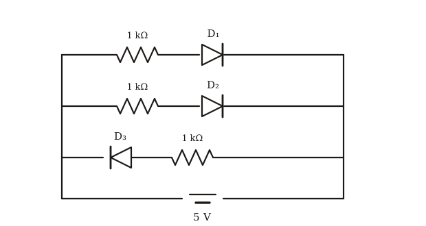
MCQ 6Direct ApplicationPractice

A diode carries 5.0 mA at a forward voltage of 0.70 V and 15.0 mA at 0.75 V. Its dynamic resistance in this interval is

Show answer and why every option is right or wrong

Answer: B. B is correct. Dynamic resistance is ΔV/ΔI = (0.75 − 0.70) V ÷ (15.0 − 5.0) mA = 0.05 V ÷ 1.00 × 10⁻² A = 5.0 Ω.

Why A is wrong: A is wrong because it is the static ratio V/I at the first point (0.70 V ÷ 5.0 mA = 1.4 × 10² Ω). The stem asks for dynamic resistance, which uses the changes, not the absolute values.

Why C is wrong: C is wrong because it takes ΔI as the first reading, 5.0 mA, instead of the change 15.0 − 5.0 = 10.0 mA: 0.05 V ÷ 5.0 × 10⁻³ A = 10 Ω.

Why D is wrong: D is wrong because it is the static ratio V/I at the second point (0.75 V ÷ 15.0 mA = 5.0 × 10¹ Ω), again the wrong quantity for a dynamic-resistance question.

MCQ 7Concept TrapPractice

A student claims that because the forward characteristic of a diode is a rising curve, the diode obeys Ohm's law once it is past the threshold voltage. The claim fails because

Show answer and why every option is right or wrong

Answer: B. B is correct. Ohm's law demands proportionality — a straight line through the origin. The forward branch is non-linear, so V/I changes from point to point and no single resistance describes the diode.

Why A is wrong: A is wrong because the forward current rises steeply past threshold; the claim's error is the shape of that rise, not its direction.

Why C is wrong: C is wrong because it contradicts the characteristic entirely — above threshold is precisely where large forward current flows.

Why D is wrong: D is wrong because Ohm's law is not a bias-dependent rule that switches on in reverse; the reverse branch is even less ohmic, being nearly flat.

MCQ 8CalculationPractice

A silicon diode with threshold voltage 0.70 V is placed in series with a resistor of 2.0 × 10² Ω across a 5.0 V DC supply, p-side toward the positive terminal. Treating the diode as an ideal switch that drops exactly 0.70 V once conducting, the current in the circuit is closest to

Show answer and why every option is right or wrong

Answer: C. C is correct. The diode is forward biased, so it conducts and drops 0.70 V; the resistor takes (5.0 − 0.70) V = 4.3 V, giving I = 4.3 V ÷ 2.0 × 10² Ω = 2.15 × 10⁻² A ≈ 2.2 × 10¹ mA.

Why A is wrong: A is wrong because it ignores the diode's forward drop and puts the whole 5.0 V across the resistor (5.0 ÷ 200 = 2.5 × 10¹ mA). The threshold voltage must be subtracted first.

Why B is wrong: B is wrong because it is the previous error compounded by a factor-of-ten slip in the division.

Why D is wrong: D is wrong because it assumes the diode blocks. With the p-side at the positive terminal the diode is forward biased and, since 5.0 V exceeds the 0.70 V threshold, it conducts.

Free NEET study resources

Get a structured 30-day Mechanics plan and a complete formula booklet — delivered to your inbox instantly.

Semiconductor Diode I–V: quick recall before you leave

How do you solve a Semiconductor Diode I–V question? A worked example

  1. 1

    Given

    • Supply voltage V = 6.0 V (DC)• Series resistance R = 3.0 × 10² Ω• Silicon diode, threshold voltage V_th = 0.70 V• Connection: n-side of the diode toward the positive terminal of the supply• Reverse saturation current of this diode = 5.0 µA

  2. 2

    Required

    The current in the circuit, and the voltage across the resistor.

  3. 3

    Concept

    A p-n junction conducts only when the p-side is at the higher potential. Here the n-side faces the positive terminal, so the junction is reverse biased: the depletion region widens, the barrier potential rises, and the only current is the saturated minority-carrier drift current. That current is fixed by thermal generation, not by the supply voltage.

  4. 4

    Formula

    Reverse bias: I = I₀ (reverse saturation current), independent of V_R below breakdown.
    Resistor voltage: V_R = I × R.

  5. 5

    Substitution

    I = 5.0 µA = 5.0 × 10⁻⁶ A
    V_R = (5.0 × 10⁻⁶ A) × (3.0 × 10² Ω)

  6. 6

    Calculation

    V_R = 1.5 × 10⁻³ V = 1.5 mV

    Note on exact values: the resistance and supply voltage are given measurements and carry two significant figures each; no counting numbers or mathematical constants enter this calculation, so the two-significant-figure answer follows directly from the given data.

  7. 7

    Final answer

    Current = 5.0 µA; voltage across the resistor = 1.5 mV. Essentially the entire 6.0 V appears across the diode, and the resistor is doing almost nothing.

  8. 8

    Common trap

    The reflex is to compute (6.0 − 0.70) ÷ 300 ≈ 1.8 × 10¹ mA — subtracting a threshold voltage and applying Ohm's law. That is the forward-bias procedure, applied to a circuit that is reverse biased. Read the terminal orientation before reaching for the arithmetic. A second trap: assuming that because the supply is 6.0 V rather than 2.0 V the reverse current must be three times larger. It is not — the reverse branch is flat.

  9. 9

    Similar NEET-style question

    A germanium diode of reverse saturation current 2.0 µA is connected in series with a 1.0 × 10³ Ω resistor across a 9.0 V supply, with its p-side toward the negative terminal. Find the current and the potential difference across the diode. *(Answer: 2.0 µA; approximately 9.0 V, since the resistor drops only 2.0 mV.)*

What to remember before solving Semiconductor Diode I–V questions

Junction between p-type and n-type semiconductors. Depletion layer forms; junction has built-in potential ~0.7 V (Si). Forward bias: low resistance, current flows. Reverse bias: high resistance, minimal current.

-- NCERT Class 12 Physics, Ch. 14, p. 334

Which Semiconductor Diode I–V formulas do you need for NEET?

1 formula — click to collapse

p-n diode bias regimes

Conceptual: p-n junction conducts in forward bias, blocks in reverse (until breakdown).

SymbolQuantitySI Unit
V_Fforward voltageV
V_Rreverse voltageV

Valid when

  • Single p-n junction
  • DC operation

More in Electronic Devices: 3 exam traps and mistakes · 2 formulas · 2 question patterns from its other lessons.

Semiconductor Diode I–V questions from past NEET papers

4 questions from NEET 2020, 2022, 2026. Answers verified against NTA official keys. — click to collapse

All 17 past-paper questions from Electronic Devices →

How does NEET ask about Semiconductor Diode I–V?

1 recurring pattern from past papers — click to collapse

Sources

Page numbers are the ones printed in the current NCERT textbook (2023 rationalised edition), unless marked pre-2023. The books are free at ncert.nic.in.

Report an error · Every fix is public: corrections log

Test yourself on this topic with real past-paper questions:

Practice this topic →