Logic Gates

8 MCQs1 revision card9-step worked example
Source: NCERT Electronic DevicesPYQ coverage: NEET 2021, 2022, 2023, 2024, 2025Official key: NTA-verifiedLast updated: 23 Sep 2026

Logic Gates, explained for NEET

A flat-backed, D-shaped symbol is an AND gate — unless there is a small circle at its output, in which case it is a NAND, and every entry in the output column flips. The same circle on a curved-back OR symbol makes it a NOR. Missing that circle is a high-frequency way to lose a mark here, because the misread gate still produces a complete, self-consistent truth table, so nothing feels wrong while you work.

The five gates in the syllabus, with A and B as binary inputs and Y as output:

  • AND, Y = A·B — output 1 only when both inputs are 1.
  • OR, Y = A + B — output 0 only when both inputs are 0.
  • NOT, Y = ¬A — a single input, inverted.
  • NAND, Y = ¬(A·B) — output 1 except when both inputs are 1.
  • NOR, Y = ¬(A + B) — output 0 except when both inputs are 0.

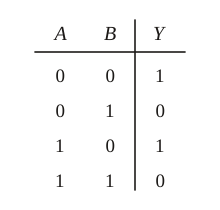
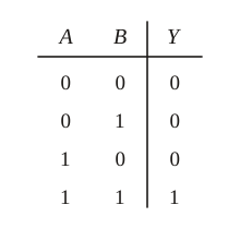
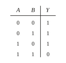
NCERT Class 12 Physics, Chapter 14, page 340 lists these truth tables together; the "except" phrasing for NAND and NOR is the fastest way to hold them.

Two consequences carry most of the exam value. First, NAND and NOR are universal: any other gate can be built from copies of either one alone. Second, joining the two inputs of a NAND or a NOR together turns it into a NOT gate — that is how an inverter appears inside circuits that seem to contain no NOT gate at all.

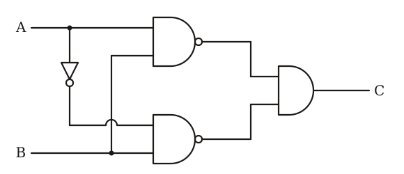
NEET asks roughly one question a year from this topic, almost always as a small circuit whose output you must trace, or a truth table you must match to a gate. Negative-marking risk is medium: the wrong option is usually the bubble-ignored answer, not a random one.

Watch-out: before writing anything, mark every bubble on the diagram. Then build all four input combinations row by row — 00, 01, 10, 11 — rather than checking the one row an option happens to mention.

Can you answer these Logic Gates MCQs?

Select an option to see the explanation. Wrong answers show why your choice was tempting — and name the exact trap it exploits.

MCQ 1Easy RecallPractice

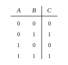
Which two-input gate produces output Y = 1 only when both inputs A and B are 1?

Show answer and why every option is right or wrong

Answer: C. The AND gate realises Y = A·B, which is 1 for the single input combination A = 1, B = 1, as given in the truth tables on NCERT Class 12 Physics, Chapter 14, page 340.

Why A is wrong: A is wrong because an OR gate gives Y = 1 whenever at least one input is 1, so it outputs 1 for three of the four combinations, not one.

Why B is wrong: B is wrong because the bubble on a NAND inverts the AND output: it gives 0 when both inputs are 1 and 1 otherwise (trap: reading NAND as AND by missing the output bubble).

Why D is wrong: D is wrong because a NOR gate gives Y = 1 only when both inputs are 0, which is the opposite input combination.

MCQ 2Easy RecallPractice

Which two gates are each, on their own, universal — meaning any other logic gate can be realised using only copies of that single gate type?

Show answer and why every option is right or wrong

Answer: A. NAND and NOR are the universal gates, since each combines an input-joining operation with an inversion; NCERT Class 12 Physics, Chapter 14, page 340 records this property alongside their truth tables.

Why B is wrong: B is wrong because neither AND nor OR can produce an inversion, so no number of them can ever build a NOT gate.

Why C is wrong: C is wrong because the question asks for gates that are universal individually: NOT alone cannot combine two inputs, and AND alone cannot invert.

Why D is wrong: D is wrong because OR cannot invert, and XOR alone cannot produce a constant needed to build the full set of gates.

MCQ 3Easy RecallPractice

The Boolean expression for a two-input NOR gate is:

Show answer and why every option is right or wrong

Answer: D. NOR is an OR followed by inversion, so Y = ¬(A + B); this is the expression listed for NOR on NCERT Class 12 Physics, Chapter 14, page 340.

Why A is wrong: A is wrong because Y = A·B is the AND gate, which has no inversion at all.

Why B is wrong: B is wrong because Y = A + B is the plain OR gate — this is the answer obtained by ignoring the bubble on the NOR symbol (trap: NOR misread as OR).

Why C is wrong: C is wrong because ¬(A·B) inverts an AND, which is NAND, not NOR.

MCQ 4Direct ApplicationPractice

For a two-input NAND gate, out of the four possible input combinations, the number of combinations for which the output Y equals 0 is:

Show answer and why every option is right or wrong

Answer: B. Applying Y = ¬(A·B) to all four rows gives Y = 0 only for A = 1, B = 1, so exactly one combination yields 0, consistent with the NAND table on NCERT Class 12 Physics, Chapter 14, page 340.

Why A is wrong: A is wrong because a gate whose output is never 0 would be a constant-1 source, not a NAND; the row A = 1, B = 1 does give 0.

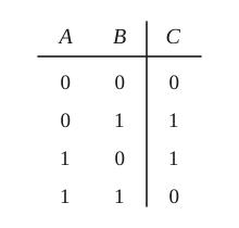
Why C is wrong: C is wrong because two zero-rows corresponds to XOR, which outputs 0 for A = B = 0 and for A = B = 1.

Why D is wrong: D is wrong because three zero-rows is the AND gate's count — this is the answer obtained when the NAND's output bubble is missed and the table is written for AND (trap: gate symbol misread).

MCQ 5Direct ApplicationPractice

The output of a two-input AND gate is fed into the input of a NOT gate. The combination is equivalent to a single:

Show answer and why every option is right or wrong

Answer: D. Inverting A·B gives ¬(A·B), which is exactly the NAND operation — the bubble on the NAND symbol represents precisely this trailing inverter, as described on NCERT Class 12 Physics, Chapter 14, page 340.

Why A is wrong: A is wrong because an OR output is 1 whenever either input is 1, whereas this circuit outputs 0 only when both inputs are 1.

Why B is wrong: B is wrong because it ignores the NOT gate entirely and reports the AND output unchanged (trap: the inversion stage dropped, the same error as missing an output bubble).

Why C is wrong: C is wrong because NOR is an inverted OR; here the first stage is an AND, not an OR.

MCQ 6Direct ApplicationPractice

Both inputs of a two-input NOR gate are joined together and a single logic input A is applied to the joined terminals. The output Y is:

Show answer and why every option is right or wrong

Answer: A. With both inputs equal to A, Y = ¬(A + A) = ¬A, so the gate behaves as an inverter — the standard way a NOT function is obtained from a universal gate, per NCERT Class 12 Physics, Chapter 14, page 340.

Why B is wrong: B is wrong because Y = A is what you get from A + A if the output bubble is ignored, i.e. treating the NOR as a plain OR (trap: inversion bubble missed).

Why C is wrong: C is wrong because for A = 1 the expression gives ¬(1 + 1) = 0, so the output is not always 1.

Why D is wrong: D is wrong because for A = 0 the expression gives ¬(0 + 0) = 1, so the output is not always 0.

MCQ 7CalculationPractice

Inputs A and B are applied to a two-input NAND gate. The output of that gate is then applied to both joined inputs of a second NAND gate, whose output is Y. The circuit is equivalent to a single:

Show answer and why every option is right or wrong

Answer: C. The first stage gives ¬(A·B); the second NAND, with its inputs joined, acts as an inverter, so Y = ¬(¬(A·B)) = A·B — an AND gate, built from NAND alone as the universality property on NCERT Class 12 Physics, Chapter 14, page 340 implies.

Why A is wrong: A is wrong because an OR from NAND gates requires the inputs to be inverted first, not the output; here only the final stage inverts.

Why B is wrong: B is wrong because NOR would demand a further inversion of an OR output, whereas double inversion here restores A·B.

Why D is wrong: D is wrong because XOR needs four input-dependent terms; this two-stage circuit produces the single product A·B.

MCQ 8Concept TrapPractice

A student is shown a gate whose symbol has the curved-back shape of an OR gate with a small circle drawn at its output. For inputs A = 0 and B = 0 the student writes the output as 0. The correct output, and the reason, are:

Show answer and why every option is right or wrong

Answer: B. The circle is the inversion indicator, so an OR shape with an output bubble is a NOR gate: Y = ¬(A + B) = ¬(0 + 0) = 1, matching the NOR table on NCERT Class 12 Physics, Chapter 14, page 340.

Why A is wrong: A is wrong because it reads the symbol as a plain OR and ignores the bubble — this is exactly the value the student obtained (trap: NOR misread as OR through a missed inversion bubble).

Why C is wrong: C is wrong because an output bubble inverts the combined result; it does not make the gate track one input.

Why D is wrong: D is wrong because the numerical value is right but the stated rule is not: a NOR outputs 1 only when no input is 1, and here both inputs are 0.

Free NEET study resources

Get a structured 30-day Mechanics plan and a complete formula booklet — delivered to your inbox instantly.

Logic Gates: quick recall before you leave

How do you solve a Logic Gates question? A worked example

  1. 1

    Given.

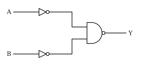
    Input A passes through a NOT gate to give ¬A. Input B passes through a separate NOT gate to give ¬B. These two inverted signals are then applied to the two inputs of a NAND gate, whose output is Y. Inputs A and B are binary logic levels, each either 0 or 1.

  2. 2

    Required.

    The complete truth table of Y, and the name of the single gate this circuit is equivalent to.

  3. 3

    Concept.

    A bubble or a NOT stage inverts the signal it sits on. Inverting both inputs of a gate is not the same as inverting its output — this is the distinction De Morgan's relations formalise, and it is the reason NAND and NOR can stand in for every other gate.

  4. 4

    Formula.

    NOT: Y = ¬A. NAND: Y = ¬(A·B). Combining the stages: Y = ¬( (¬A) · (¬B) ).

  5. 5

    Substitution.

    Evaluate the expression row by row, over all four input combinations, keeping the intermediate column ¬A·¬B visible:

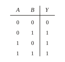
    | A | B | ¬A | ¬B | ¬A·¬B | Y = ¬(¬A·¬B) |
    |---|---|----|----|-------|--------------|
    | 0 | 0 | 1 | 1 | 1 | 0 |
    | 0 | 1 | 1 | 0 | 0 | 1 |
    | 1 | 0 | 0 | 1 | 0 | 1 |
    | 1 | 1 | 0 | 0 | 0 | 1 |

  6. 6

    Calculation.

    The output column reads 0, 1, 1, 1 — it is 0 only for A = 0, B = 0 and 1 for every other combination. All quantities here are exact binary logic levels (0 and 1) and are dimensionless, so no significant-figure or rounding consideration applies to any entry in this table.

  7. 7

    Final answer.

    Y = A + B. The circuit — two inverters feeding a NAND — is equivalent to a single OR gate.

  8. 8

    Common trap.

    The bubble on the NAND symbol sits on its output, and the two NOT gates sit on its inputs; these do not cancel to give a plain AND. A student who mentally strips all three inversions writes Y = A·B and reads the output column as 0, 0, 0, 1 — wrong in three of the four rows, though it looks like a complete answer. Mark every bubble and every NOT stage on the diagram before you write the first row, and keep the intermediate column as a check.

  9. 9

    Similar NEET-style question.

    Inputs A and B are applied to a NOR gate, and the NOR output is passed through a NOT gate to give Y. Construct the truth table for Y and identify the equivalent single gate. *(Answer: Y = A + B, an OR gate — the NOT restores what the NOR's bubble inverted.)*

What to remember before solving Logic Gates questions

In the NEET syllabus; removed from current NCERT.

In digital circuits only two values (0 or 1) of input and output voltage are permissible. NOT gate: output is the inverse of the input. OR gate: output Y is 1 when either input A or input B or both are 1. AND gate: output Y is 1 only when input A and input B are both 1. NAND gate: an AND gate followed by a NOT gate. NOR gate: a NOT operation applied after an OR gate; output Y is 1 only when both inputs A and B are 0. NAND gates are also called universal gates, and NOR gates are considered universal gates because all the gates like AND, OR, NOT can be obtained by using only NOR gates.

-- NCERT Class 12 Physics (pre-2023 edition), Chapter 14, p. 491
Which Logic Gates formulas do you need for NEET?

1 formula — click to collapse

Common logic gate truth tables

Boolean operations on binary inputs. NAND and NOR are universal gates.

SymbolQuantitySI Unit
A, Bbinary inputs (0 or 1)-
Ybinary output (0 or 1)-

Valid when

  • Binary digital logic
  • Ideal gates (no propagation delay considered)

Where do students lose marks on Logic Gates?

These are the exact patterns that cause wrong answers in NEET. Each trap includes when it triggers and how to avoid it.

2 items — click to collapse

Category: Similar Terms

Student misreads NAND as AND or NOR as OR. The 'bubble' on the output of NAND/NOR is the negation indicator.

When it triggers

Truth table or logic circuit identification problem.

How to avoid

Check for output bubble. AND with bubble = NAND. OR with bubble = NOR. NAND truth table: outputs 1 EXCEPT when both inputs are 1.

More in Electronic Devices: 1 exam trap or mistake · 2 formulas · 2 question patterns from its other lessons.

How does NEET ask about Logic Gates?

1 recurring pattern from past papers — click to collapse

Sources

NCERT refs: Class 12 Physics Chapter 14, p.340

Page numbers are the ones printed in the current NCERT textbook (2023 rationalised edition), unless marked pre-2023. The books are free at ncert.nic.in.

Report an error · Every fix is public: corrections log

Test yourself on this topic with real past-paper questions:

Practice this topic →